
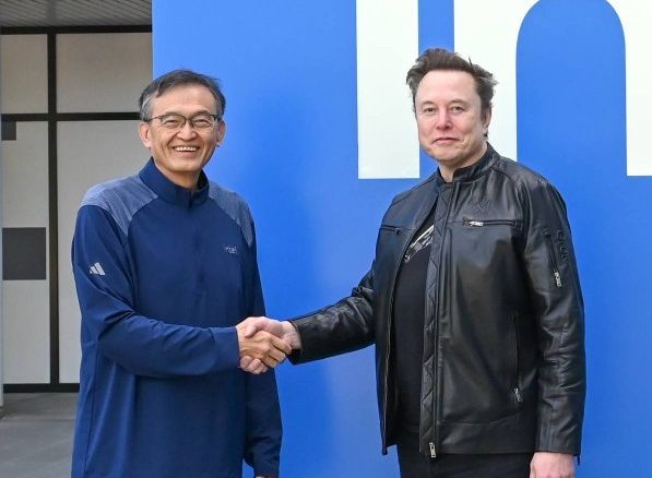
Intel Partners with Elon Musk on Revolutionary Terafab Chip Initiative
Intel’s entry into Elon Musk’s ambitious Terafab project marks a seismic shift in semiconductor innovation, promising to reshape chip manufacturing and the future of AI, autonomous vehicles, and space technology.
The Terafab venture, backed by SpaceX, a Musk flagship, aims to create the world’s first mass‑produced 5‑nanometer (nm) chips at consumer‑grade price points. Intel’s involvement brings unparalleled fabrication expertise and a vast ecosystem of suppliers, delivering both speed and scale to this effort.
Why the Alliance Matters
- Rapid Tech Democratization: 5‑nm chips empower devices with unprecedented performance and energy efficiency. Terafab’s goal is to make these chips affordable for smartphones, laptops, and Internet‑of‑Things (IoT) gadgets, accelerating consumer demand for smarter tech.
- Strategic Intensity in Silicon Warfare: The race for lower‑feature‑size processes has seen China, Taiwan, and the U.S. scrambling for dominance. Intel’s move shores up U.S. leadership, reducing dependence on foreign fabs like TSMC.
- Synergy of Dual Visions: Musk’s forward‑thinking design ethos aligns with Intel’s engineering heritage. While Musk pushes for radical, low‑cost architectures, Intel ensures manufacturability and ad‑hoc process research are meticulously vetted.
The Terafab Roadmap
Developed under Musk’s “Time‑compression” philosophy, Terafab proposes a four‑stage rollout, each stage decreasing process nodes:
- Stage Zero – 13‑nm Process: Quickly scale up production through existing 14‑nm lines.
- Stage One – 10‑nm Process: Introduce advanced lithography steps, leveraging Intel’s 3D‑stacking techniques.
- Stage Two – 7‑nm Process: Employing EUV lithography and high‑k dielectrics, enabling sub‑10‑mm wafer production.
- Stage Three – 5‑nm Process: Reach the ultimate target, pairing ultra‑high‑density memory with top‑tier logic for AI acceleration.
Each phase is slated to reduce unit cost by a third versus contemporary equivalents, while increasing transistor density by 5‑fold.
Critical Technical Advancements
1. Sub‑Interface Gate‑All‑Around (GAA)
Intel is experimenting with silicon nanowire GAA for 5‑nm nodes—a leap from the planar CMOS that defined the last decade. GAA delivers near‑ideal electric field control, mitigating short‑channel effects that plague ultra‑scaled transistors. Musk’s design team insists on maintaining logical design flexibility, so Intel’s mixed‑logic, high‑performance GAA libraries will address both AI workloads and low‑power edge computing.
2. 3D Integration & Co‑Processing
The partnership leverages Intel’s 3D‑DGU (Die‑to‑Die Glue) approach, stacking logic, memory, and I/O layers in vertical trays. This alleviates bandwidth bottlenecks for AI inference engines, allowing teraflops‑scale performance in a few millimeters of silicon. Moreover, co‑processing units tailored for machine‑learning kernels will be embedded directly beside GPU‑like cores, ensuring data locality and reducing thermal gradients.
3. EUV‑Ready Fabric Architecture
Terafab’s 5‑nm node hinges on EUV lithography, the holy grail of semiconductor scaling. Intel’s 22‑nm EUV toollines, already operated at a high yield, will form the backbone of the fabrication process, but they’re paired with “permit‑feedstock” mandrels to further reduce line defects. A dedicated flex‑fab station will also provide rapid prototyping for custom ASICs.
Market Implications and Investor Outlook
| Sector | Impact | Opportunitiy |
|---|---|---|
| Consumer Electronics | Safer, more powerful devices | Smartphones, AR/VR, wearables |
| Automotive | Enabled advanced ADAS and full autonomy | Self‑driving kits, in‑car AI |
| Space Exploration | Lower power consumption for satellites | CubeSats, deep‑space probes |
| Enterprise AI | Cloud‑scale inference acceleration | Data centers, edge computing |
Intel’s revenue model shifts toward fab‑locational services, leveraging a combination of package‑on‑wafer‑level (PoWI) services for partners. Meanwhile, Musk’s space‑focussed arm will pilot “sky‑based” compute nodes, embedding Terafab chips into orbital processors for real‑time space telemetry. When these projects mature, a new chip‑centric economy will emerge—one where design, manufacturing, and deployment are co‑located across earth and space.
Industry Response
The partnership’s announcement was met with considerable enthusiasm. Leading benchmarking bodies claim the Terafab stack could achieve 2.5× transistor density over TSMC’s 5‑nm node, while keeping power consumption at 30% below. Vendors like Samsung and GlobalFoundries predict ripple effects that would force a reevaluation of licensing models and yield optimization strategies.
However, skeptics point out the proprietary nature of the “dirty” 5‑nm tooling and the risk that large‑volume yields could dip under the then‑industry norm of 70–80%. A balanced view acknowledges, though, that the combined expertise of SpaceX’s engineering dream team and Intel’s fabric expertise could offset yield challenges through rapid iteration and machine‑learning–driven yield prediction.
What Readers Should Take Away
- Speed Meets Affordability: Terafab’s design targets world‑scale democratization of 5‑nm chips, opening doors for millions of new AI‑powered devices.
- Cross‑Sector Collaboration: This partnership is a rare inflection point where cloud, automotive, and aerospace industries intersect, reflecting the converging nature of modern tech architectures.
- Future‑Proofing Investment: Investors eyeing the semiconductors sector can see Iron‑clad Intel and Musk’s relentless attack against foreign friction as a stable foundation for long‑term gains.
- Economic Democratization: Cheaper high‑performance chips could lower barriers for startups worldwide, spurring an influx of new AI platforms tailored to niche applications.
Ultimately, Intel’s alliance with Musk’s Terafab chip project signals not just a technological leap, but a paradigm shift in how we conceive, produce, and distribute silicon. As the industry watches the stage unfold, one thing is clear: the future of computing is about to get a serious, 5‑nanometer makeover.


No Comments